Context#
In April 2023 my wonderful wife had the best birthday idea ever, and made me a custom development board based on an STM32H7 MCU.
The chip was rather cool and had an USB connector, an SD-card interface, and a JLink connector. It was all I needed at the time.
As it was my first time selecting a processor, I just cared about the CPU architecture, presence of caches, and clock frequency. I didn’t request a large flash or RAM size.
This detail ended up causing me some troubles, as I “quickly” (in a few months of adding code and developing a Kasan that needed a lot more code) filled the 128KiB of builtin Flash.
I then decided to upgrade the CPU, and since new capabilities are never worth nothing, I attempted to design the devboard V2 myself.
During this year of development, I also had written a custom USB stack and a driver to support ST’s USB implementation. And if it doesn’t sound hard, trust me, it is. ST’s USB module is the biggest pile of hardware crap I ever encountered. It had it all. Undocumented registers, hardware xprop, sudden freezes for no reasons, almost undocumented HW capabilities, pseudo-documented capabilities that aren’t actually implemented, name it and it had it. I bumped my head on the wall so much during the month and a half where I wrote that code, that the noise still resonates in the place that my now liquified brains used to occupy.
But that’s another story.
An USB stack I had, and I wanted to experiment with it. More precisely, I wanted to try using an USB-C connector instead of my old USB-B, and also wanted to give High Speed USB a try, because ST’s Full Speed USB wasn’t painfully broken enough.
I also wanted to try and support the Ethernet, since there could be a lot more fun places where ST could fuck up, so why not visiting them all !
I also wanted to experiment more on smaller peripherals, like I2C, UARTs et al., and I wanted dedicated connectors on the board for them because why not.
Pin multiplexing#
An SoC is essentially one or more CPUs and multiple peripherals connected together via various interconnects.
While CPUs are essentially processing data, peripherals sometimes use signals from the outer world. For example, an UART will have at least two signals, RX and TX, and likely have one control-flow signal per direction, which will add two more pins, CTS (Clear to Send) and RTS (Request to Send).
That’s already 4 signals, for a single peripheral. And that’s a rather low number of signals : memory access peripherals use data buses which use at least 8 signals (one byte), plus the various DIR/CLK signals.
Now imagine that we have 10 UART peripherals on the chip, that’s already 40 pins used. Add the various SPI, I2C that may be present, the LCD peripherals, and so on, and you easily end up with hundreds or thousands of pins.
A normal chip package doesn’t have that many pins : the LQFP-144, which is already a big one, only has 144 pins as the name states.
It simply cannot allow all peripherals to be used at the same time.
How is this not a problem then ? Well, simply because typical applications do not use all those peripherals.
Thanks to this, MCU manufacturers like ST have come up with a reasonable approach that we’ll call pin multiplexing : every pin of the package is internally connectable to multiple signals (but to at most one at a time). The GPIO driver has to configure which alternate function (which index of each pin’s multiplexer) is used. This is one of the first duties of any communication (USB, UART, etc…) device driver of such a chip : configure the pin multiplexing so that the signals used by the driven device are actually connected to the chip’s pins. Then it can do other fun(damental) things like configuring the clocks and generating kernel panics.
The multiplexer can be large though. For ST’s H7 line, it is 16 entries wide, meaning that each pin can be internally connected to at most 16 signals.
But the fun goes the other way too : multiple pins can be connected to the same signal, which makes this connection system a good old nightmare-ish graph.
To see how deep out of fun-land we are, this is an excerpt from my chip’s multiplexing array.
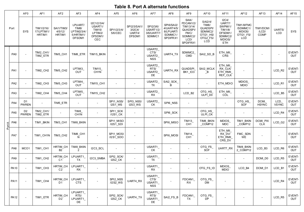
This can be (painfully) translated into a machine readable text file that we’ll use later.
For the record, that took almost 3 days of part-time fun and cost me a few neurons.
The sytax is quite simple and doesn’t deserve a detailed explanation, it’s just a line by line description where the first non whitespace char determines the described entity.
It could be possible to directly get this information from the pdf using a pdf-to-text-like manner. Though I tried that for a couple of hours and quickly ran out of patience.
The problem#
Now back to our original problem : a devboard I wanted to design. And I knew what I wanted :
- 4 UARTs, among 8.
- 3 SPIs, among 6.
- 2 I2Cs, among 4.
- 1 CAN, among 2.
- 1 4 bit SD interface, among 2.
- 1 USB with an ULPI interface, only 1 in the chip.
- 1 USB with a standard FS interface, only 1 in the chip.
- 1 Ethernet MDC + RMII interface, only 1 in the chip.
When I say ‘among’ in the list above, I mean that there are many devices of a kind in the SoC, but that I only want a certain number of them. Those devices are, for all intents and purposes, strictly identical. Any of those can be selected.
The issue, as one could imagine, is that because the total number of pins is pretty low, and the number of signals is pretty high, there is a high chance of collision.
Now, if you think about it, I could just have try-and-errored in Kicad until I found a valid solution : if I saw that one peripheral needed one pin that was used by another, I would have discarded the one with the smallest priority and repeated the process.
As a matter of fact, I did try that. And it gets old. Veeeeeeryyyyyy quickly.
That’s mostly because if you think about it for a moment, there are a LOT of possible combinations : let’s imagine that we know exactly every peripheral that we need (forget the M among N-s in the previous list), and that we have 16 of them. Every one of them has 4 signals, and each signal can be routed to 2 pins. We literally have 64 pins that each have two possible values, which makes a total of 2^64 possible configurations.
And that’s a lot. More than what your computer can index.
And doing that manually can be very long.
So after the first evening of failed attempts with the donk-ish manual way, I told myself it would be great to use the few remaining connected neurons to at least code something to accelerate the process.
Objective#
With a given problem (certain peripherals to select) there could be a lot of possible solutions.
The objective of the algorithm will not be to find all solutions, not because it would be a bad idea, but simply because it would potentially consume all disk space on the machine.
In fact, as the reader will see, the resolution method contains the procedure to find all possible solutions. It is just that in most cases, finding just one solution is enough.
Thus, the objective of the algorithm will be to find one solution. If for some reason, that solution is not what the user expects, then the algorithm will easily find the next possible solutions.
The expected output#
Ideally, we would like to be able to iteratively test multiple solutions for the same problem, in the same design.
To do that, we would like our algorithm to modify the connections in our Kicad schematics.
This is not doable per-se, but can be accomplished by structuring our Kicad schematics like the following :
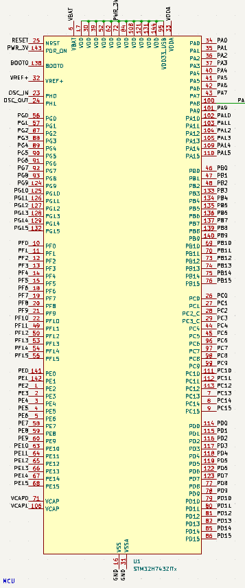
The microcontroller only has labels connected to its GPIO pins, like what follows.
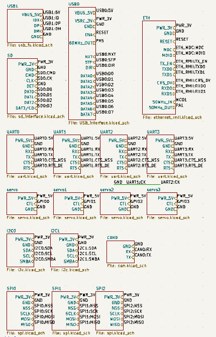
All the hardware connected to the GPIO pins (USB physical layer, ethernet PHY chip, UART connectors, etc…) only has labels connected to its signal pins, like what follows.
Then, the only remaining thing is for our algorithm to generate a label associative array that for each GPIO pin of the microcontroller, connects to a hardware label, or to to GPIOs if the pin is not used like follows.
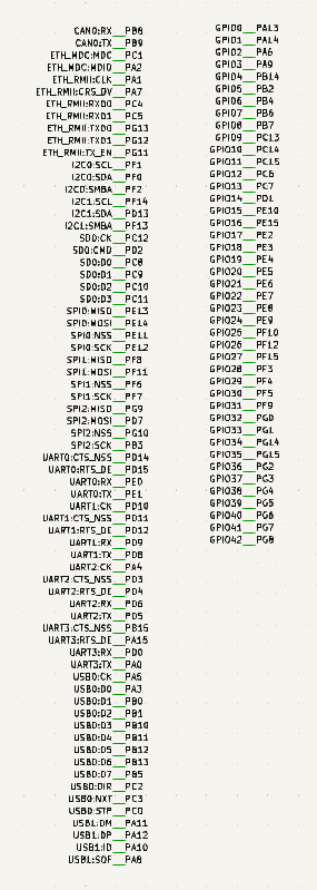
Luckily, Kicad uses text-based representations for the schematic components of a design, which allows us to copy-paste them. We will use that in a hacky manner, and make our algorithm generate the text representation of a label connection array.
Here is the one for the previous image.
We will then copy paste that into kicad’s schematics editor and that will be it.
Numerical complexity#
There are two factors that cause the numerical complexity of the problem to exponentially increase : signals being connected to multiple pins, and us wanting to choose “K peripherals in a set of N”.
Let’s formally establish the number of possible combinations that we should theoretically test.
First, each signal sig can be connected to multiple pins pin_nb(sig).
Each peripheral per uses the set of signals per_sigs(per).
Then, for each group grp (ex UART) of peripherals that we must use, we have per_nb(grp) peripherals available for that group and we must pick chosen_nb(grp) in that group.
Each group grp has per_nb(grp) choose chosen_nb(grp) possible configurations, with n choose k = n! / (k! * (n - k)!).
Each configuration uses the set of peripherals cfg_pers(cfg).
The total number of possible combinations to test can be written the following way :
N = PROD(grp in grps){ SUM(cfg in cfgs(grp)) { PROD(per in cfg_pers(cfg)) { PROD(per_sigs(per)) {pin_nb(sig)} } } }
Theoretically, we could just iterate over all those combinations, check if each is valid, and stop at the first valid one.
Though, if our model has a lot of peripherals with a lot of signals, we could iterate over a lot of combinations before finding a valid one.
In order for that search to be quicker, there are a few optimizations that we can do. During the development of this project, I was using a template design / peripheral selection as an example, and those optimizations made the number of potential solutions go from more than 2 ^ 64 to actually 16.
Not 2 ^ 16. I actually mean 16 combinations to try.
Algorithmic data structures#
The first thing we must do is translate the pin multiplexing array in the microcontroller’s doc into a machine readable text file that our algorithm will process.
That is long and painful, but trust me, it’s worth it. It is very likely that all chips in the same family (ST’s H7 for example) share the same multiplexing layout, so you may not have to do that frequently.
Then we can read this file, and build a graph-like in-ram data structure, where :
- each group references its possible configurations (k choose n)
- each configuration references its peripherals.
- each peripheral references its signals.
- each signal references its pins.
Here one must note :
- each configuration is part of one and exactly one group.
- each peripheral can be referenced by multiple configurations of the same group. (A)
- each signal is part of one and exactly one peripheral.
- each pin can be referenced by multiple signals. (B)
A and B are the two factors that were previously mentioned to make the complexity explode.
Those are the places where we must optimize things, by reducing the exploration space. Though, we cannot afford to remove a potential solution for the sake of speed. We must ensure that we only remove invalid configurations from the exploration space.
Peripheral types#
In the next sections, when the expression “for exploration purposes” or “FEP” is used, it means “given the current optimizations we found for the exploration”. For example, a signal S can be connectable to a pin P, that is guaranteed to be connected to another signal in every valid combination. In this case, S will be considered disconnected from P for exploration purposes.
First, we can note that some peripherals are optional and some are mandatory :
- if a peripheral is part of a group where all peripherals will be chosen (FEP) (i.e. we choose N peripherals in a set of N, which is equivalent to having a group for each) then it is mandatory (FEP), in the sense that if a valid combination exists, this peripheral will be part of it.
- otherwise, the peripheral is optional FEP in the sense that if a valid combination exists, it may or may not be part of it.
If a peripheral is mandatory, then we can start to optimize its signals.
Signals optimizations#
If a peripheral is mandatory, so are its signals. That means that if such a signal S can only be connected to one pin P, then it must be connected to it.
Other signals of other peripherals connected to this pin can just be considered not connected to it for exploration purposes, since if there is a valid configuration, S will be connected to P.
If a signal is found to be connected to no pin for exploration purposes (i.e all its possible pins are known to be connected to other signals), it means that the related peripheral cannot be present in the final solution, and that we can just remove this peripheral from the graph.
If the peripheral is mandatory, then no solution exists.
If the peripheral is optional, then we can actually remove it from the graph.
If we find a signal to be connected to multiple pins, and one of those pins P is connected to no other signal, then we can disconnect the signal connected to P and disconnect it from all other signals.
This effectively reduces the number of connections on other pins, which potentially allows us to re-apply the first optimization discussed above.
Signals optimizations#
If the peripheral is optional, then we can remove it from the exploration space (i.e. from the graph). This has two consequences.
First, every signal that we remove removes a connection to the pin that it was previously connected to. This potentially creates new pins with a single connection and we can re-apply the signal optimization sequence.
Then, every peripheral that we remove is optional, and thus, is part of a group where we chose K peripherals among N, with K < N. Removing the peripheral reformulates the problem, by forcing us to choose K peripherals among N - 1 peripherals.
If K == N - 1, then all remaining peripherals become mandatory, and we can optimize them all using signal optimizations.
If K < N - 1, then all remaining peripherals are still optional.
In order to simplify the exploration space, we apply the signal optimizations and peripheral removal procedures repeatedly to the graph, until it leaves the graph unaffected.
Then, we can bruteforce the graph by testing the validity of all remaining combinations.
Pathological case#
There is a case where those optimisations bring no improvement.
Let’s imagine a simple scenario where we have 2 pins on our SOC, we want to select 2 mandatory peripherals, each peripheral has 1 signal that can be connected to both pins.
No optimization will work here, since each pin is connectable to 2 signals, and each signal is connectable to 2 pins.
Thus, those optimizations will not always improve performance, but they will statistically improve it a lot, since this kind of pathological case is rather rare, or only involves a low number of pins.